Wednesday, December 5, 2018

Network Devices (Hub, Repeater, Bridge, Switch, Router, Gateways and Brouter)

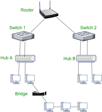
1. Repeater – A repeater operates at the physical layer. Its job is to regenerate the signal over the same network before the signal becomes too weak or corrupted so as to extend the length to which the signal can be transmitted over the same network. An important point to be noted about repeaters is that they do not amplify the signal. When the signal becomes weak, they copy the signal bit by bit and regenerate it at the original strength. It is a 2 port device.

2. Hub –  A hub is basically a multiport repeater. A hub connects multiple wires coming from different branches, for example, the connector in star topology which connects different stations. Hubs cannot filter data, so data packets are sent to all connected devices.  In other words, collision domain of all hosts connected through Hub remains one.  Also, they do not have intelligence to find out best path for data packets which leads to inefficiencies and wastage.
Types of Hub

  • Active Hub :- These are the hubs which have their own power supply and can clean , boost and relay the signal along the network. It serves both as a repeater as well as wiring center. These are used to extend maximum distance between nodes.
  • Passive Hub :- These are the hubs which collect wiring from nodes and power supply from active hub. These hubs relay signals onto the network without cleaning and boosting them and can’t be used to extend distance between nodes
3. Bridge – A bridge operates at data link layer. A bridge is a repeater, with add on functionality of filtering content by reading the MAC addresses of source and destination. It is also used for interconnecting two LANs working on the same protocol. It has a single input and single output port, thus making it a 2 port device.

Types of Bridges

  • Transparent Bridges :- These are the bridge in which the stations are completely unaware of the
    bridge’s existence i.e. whether or not a bridge is added or deleted from the network , reconfiguration of
    the stations is unnecessary. These bridges makes use of two processes i.e. bridge forwarding and bridge learning.
  • Source Routing Bridges :- In these bridges, routing operation is performed by source station and the frame specifies which route to follow. The hot can discover frame by sending a specical frame called discovery frame, which spreads through the entire network using all possible paths to destination.

4. Switch – A switch is a multi port bridge with a buffer and a design that can boost its efficiency(large number of  ports imply less traffic) and performance. Switch is data link layer device. Switch can perform error checking before forwarding data, that makes it very efficient as it does not forward packets that have errors and  forward good packets selectively to correct port only.  In other words, switch divides collision domain of hosts, but broadcast domain remains same.

5. Routers – A router is a device like a switch that routes data packets based on their IP addresses. Router is mainly a Network Layer device. Routers normally connect LANs and WANs together and have a dynamically updating routing table based on which they make decisions on routing the data packets. Router divide broadcast domains of hosts connected through it.

img1

6. Gateway – A gateway, as the name suggests, is a passage to connect two networks together that may work upon different networking models. They basically works as the messenger agents that take data from one system, interpret it, and transfer it to another system. Gateways are also called protocol converters and can operate at any network layer. Gateways are generally more complex than switch or router.

7. Brouter – It is also known as bridging router is a device which combines features of both bridge and router. It can work either at data link layer or at network layer. Working as router, it is capable of routing packets across networks and working as bridge, it is capable of filtering local area network traffic.
References https://en.wikipedia.org/wiki/Gateway_%28telecommunications%29

Monday, November 12, 2018

Difference Between PLA and PAL


Difference Between PLA and PAL

PLA and PAL are types of Programmable Logic Devices (PLD) which are used to design combination logic together with sequential logic. The significant difference between the PLA and PAL is that the PLA consists of the programmable array of AND and OR gates while PAL has the programmable array of AND but a fixed array of OR gate. PLD’s provides a more simple and flexible way of designing the logic circuits where the number of functions can also be increased. These are also implemented in IC

Before PLD’s, multiplexers were used for designing a combinational logic circuit, these circuits were highly complex and rigid. Then Programmable logic devices(PLD) are developed, and the first PLD was ROM. ROM design was not very successful as it emerged the issue of hardware wastage and increasing exponential growth in the hardware for every large application. To overcome the limitations of ROM, PLA and PAL were devised. PLA and PAL are programmable and effectively utilizes the hardware

Comparison Chart
BASIS FOR COMPARISONPLAPAL
Stands forProgrammable Logic ArrayProgrammable Array Logic
ConstructionProgrammable array of AND and OR gates.Programmable array of AND gates and fixed array of OR gates.
AvailabilityLess prolificMore readily available
FlexibilityProvides more programming flexibility.Offers less flexibility, but more likely used.
CostExpensiveIntermediate cost
Number of functionsLarge number of functions can be implemented.Provides the limited number of functions.
SpeedSlowHigh
Definition of PLA

PLA stands for the Programmable Logic Array which presents the boolean function in the SOP (Sum of Products) form. The PLA contains NOT, AND and OR gates fabricated on the chip. It passes every input by a NOT gate which makes each input and its complement available to every AND gate. The output of each AND gate is given to the each OR gate. At last, the OR gate output produces chip output. So, this is how suitable connections are made to employ SOP expressions


In PLA the connections to both AND and OR arrays are programmable. PLA is considered more expensive and complex as compared to the PAL. The two different manufacturing techniques can be used for PLA to increase the ease of programming. In this technique, each connection is built through a fuse at every intersection point where the unwanted connections can be removed by blowing the fuses. The latter technique involves the connection making at the time of the fabrication process with the help of the proper mask provided for the specific interconnection pattern.
Definition of PAL

PAL (Programmable Array Logic) 
                                                              PAL is also a PLD (Programmable Logic Device) circuit which works similar to the PLA. PAL employs the programmable AND gates but fixed OR gates, unlike PLA. It implements two simple functions where the number of linked AND gates to each OR gate specifies the maximum number of product terms that can be generated in a sum-of-products representation of the particular function. While the AND gates are perpetually connected to the OR gates, which signifies that the produced product term is not shareable with the output functions


The main concept behind developing PLD’s is to embed a complex boolean logic into a single chip. Therefore, eliminating the unreliable wiring, preventing the logic design and minimizing power consumption.


Key Differences Between PLA and PAL

  • The PLA is PLD, comprised of two levels of programmable logic AND plane and OR plane. On the other hand, PAL contains only programmable AND plane and fixed OR plane.
  • When it comes to availability, the PAL is more readily available along with easy production. In contrast, the PLA is not easily available.
  • The PLA is more flexible than a PAL.
  • PLA is costlier as compared to the PAL.
  • A number of functions provided by PLA are more relatively because it enables the programming of the OR plane also.
  • PAL works faster while PLA is slower comparatively.

Conclusion


Programmable Logic Array (PLA) and Programmable Array Logic (PAL) are the PLD (Programmable Logic Devices) where PLA is more adaptable and flexible than PAL. However, PAL can easily produce a combination logic circuit.

UNIT-5 MATERIAL

Micro-Operations


Micro-Operations

The operations executed on data stored in registers are called micro-operations. A micro-operation is an elementary operation performed on the information stored in one or more registers.

Example: Shift, count, clear and load.

Types of Micro-Operations

The micro-operations in digital computers are of 4 types:

Register transfer micro-operations transfer binary information from one register to another.

1)Arithmetic micro-operations perform arithmetic operations on numeric data stored in registers

2)Logic micro-operations perform bit manipulation operation on non-numeric data stored in registers.

3)Shift micro-operations perform shift micro-operations performed on data.

Arithmetic Micro-Operations

Some of the basic micro-operations are addition, subtraction, increment and decrement.

Add Micro-Operation

It is defined by the following statement: 

R3 → R1 + R2

The above statement instructs the data or contents of register R1 to be added to data or content of register R2 and the sum should be transferred to register R3.

Subtract Micro-Operation

Let us again take an example: R3 → R1 + R2' + 1

In subtract micro-operation, instead of using minus operator we take 1's compliment and add 1 to the register which gets subtracted, i.e R1 - R2 is equivalent to R3 → R1 + R2' + 1

Increment/Decrement Micro-Operation

Increment and decrement micro-operations are generally performed by adding and subtracting 1 to and from the register respectively.

R1 → R1 + 1
R1 → R1 – 1

Symbolic Designation            Description

R3 ← R1 + R2                       Contents of R1+R2 transferred to R3.
R3 ← R1 - R2                        Contents of R1-R2 transferred to R3.
R2 ← (R2)'                            Compliment the contents of R2.
R2 ← (R2)' + 1                      2's compliment the contents of R2.
R3 ← R1 + (R2)' + 1             R1 + the 2's compliment of R2 (subtraction).
R1 ← R1 + 1                         Increment the contents of R1 by 1.
R1 ← R1 - 1                          Decrement the contents of R1 by 1.

Logic Micro-Operations

These are binary micro-operations performed on the bits stored in the registers. These operations consider each bit separately and treat them as binary variables.

Let us consider the X-OR micro-operation with the contents of two registers R1 and R2.
P: R1 ← R1    X-OR     R2

In the above statement we have also included a Control Function.

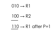
Assume that each register has 3 bits. Let the content of R1 be 010 and R2 be 100. The X-OR micro-operation will be:


Shift Micro-Operations

These are used for serial transfer of data. That means we can shift the contents of the register to the left or right. In the shift left operation the serial input transfers a bit to the right most position and in shift right operation the serial input transfers a bit to the left most position.

There are three types of shifts as follows:

a) Logical Shift

It transfers 0 through the serial input. The symbol "shl" is used for logical shift left and "shr" is used for logical shift right.

R1 ← she R1
R1 ← she R1

The register symbol must be same on both sides of arrows.

b) Circular Shift

This circulates or rotates the bits of register around the two ends without any loss of data or contents. In this, the serial output of the shift register is connected to its serial input. "cil" and "cir" is used for circular shift left and right respectively.

c) Arithmetic Shift

This shifts a signed binary number to left or right. An arithmetic shift left multiplies a signed binary number by 2 and shift left divides the number by 2. Arithmetic shift micro-operation leaves the sign bit unchanged because the signed number remains same when it is multiplied or divided by 2.

TYPES OF RAM & ROM


PROM:
               short for programmable read-only memory A PROM is a memory chip on which data can be written only once. Once a program has been written onto a PROM, it remains there forever. Unlike RAM, PROM's retain their contents when the computer is turned off. The difference between a PROM and a ROM (read-only memory) is that a PROM is manufactured as blank memory, whereas a ROM is programmed during the manufacturing process. To write data onto a PROM chip, you need a special device called a PROM programmer or PROM burner. The process of programming a PROM is sometimes called burning the PROM. 

EPROM:- (erasable programmable read-only memory) is a special type of PROM that can be erased by exposing it to ultraviolet light. Once it is erased, it can be reprogrammed. An EEPROM is similar to a PROM, but requires only electricity to be erased. 

EEPROM- Acronym for electrically erasable programmable read-only memory. Pronounced double-ee-prom or e-e-prom, an EEPROM is a special type of PROM that can be erased by exposing it to an electrical charge. Like other types of PROM, EEPROM retains its contents even when the power is turned off. Also like other types of ROM, EEPROM is not as fast as RAM. EEPROM is similar to flash memory (sometimes called flash EEPROM). The principal difference is that EEPROM requires data to be written or erased one byte at a time whereas flash memory allows data to be written or erased in blocks. This makes flash memory faster.

RAM (Random Access Memory) is a temporary (Volatile) storage area utilized by the CPU. Before a program can be ran the program is loaded into the memory which allows the CPU direct access to the program. 

2 Types of RAM

SRAM Short for static random access memory, and pronounced ess-ram. SRAM is a type of memory that is faster and more reliable than the more common DRAM (dynamic RAM). The term static is derived from the fact that it doesn't need to be refreshed like dynamic RAM. 

SRAM is often used only as a memory cache usually found in the CPU (L1, L2 and L3 Cache)

DRAM stands for dynamic random access memory, a type of memory used in most personal computers.

Computer Memory


Memory Organization in Computer Architecture


A memory unit is the collection of storage units or devices together. The memory unit stores the binary information in the form of bits. Generally, memory/storage is classified into 2 categories: 

Volatile Memory: This loses its data, when power is switched off. 

Non-Volatile Memory: This is a permanent storage and does not lose any data when power is switched off. 

Memory Hierarchy


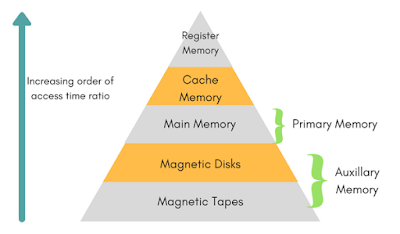
The total memory capacity of a computer can be visualized by hierarchy of components. The memory hierarchy system consists of all storage devices contained in a computer system from the slow Auxiliary Memory to fast Main Memory and to smaller Cache memory.

Auxillary memory access time is generally 1000 times that of the main memory, hence it is at the bottom of the hierarchy.


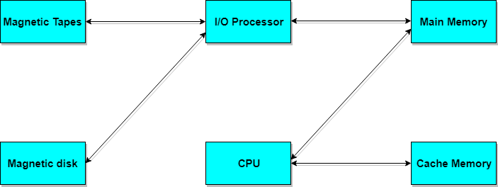
The main memory occupies the central position because it is equipped to communicate directly with the CPU and with auxiliary memory devices through Input/output processor (I/O).

When the program not residing in main memory is needed by the CPU, they are brought in from auxiliary memory. Programs not currently needed in main memory are transferred into auxiliary memory to provide space in main memory for other programs that are currently in use.

The cache memory is used to store program data which is currently being executed in the CPU. Approximate access time ratio between cache memory and main memory is about 1 to 7~10


Memory Access Methods


Each memory type, is a collection of numerous memory locations. To access data from any memory, first it must be located and then the data is read from the memory location. Following are the methods to access information from memory locations:

Random Access: Main memories are random access memories, in which each memory location has a unique address. Using this unique address any memory location can be reached in the same amount of time in any order.

Sequential Access: This methods allows memory access in a sequence or in order.

Direct Access: In this mode, information is stored in tracks, with each track having a separate read/write head.

Main Memory

The memory unit that communicates directly within the CPU, Auxillary memory and Cache memory, is called main memory. It is the central storage unit of the computer system. It is a large and fast memory used to store data during computer operations. Main memory is made up of RAM and ROM, with RAM integrated circuit chips holing the major share.

RAM: Random Access Memory

DRAM: Dynamic RAM, is made of capacitors and transistors, and must be refreshed every 10~100 ms. It is slower and cheaper than SRAM.

SRAM: Static RAM, has a six transistor circuit in each cell and retains data, until powered off.

NVRAM: Non-Volatile RAM, retains its data, even when turned off. Example: Flash memory.

ROM: Read Only Memory, is non-volatile and is more like a permanent storage for information. It also stores the bootstrap loader program, to load and start the operating system when computer is turned on. PROM(Programmable ROM), EPROM(Erasable PROM) and EEPROM(Electrically Erasable PROM) are some commonly used ROMs.

Auxiliary Memory
Devices that provide backup storage are called auxiliary memory. For example: Magnetic disks and tapes are commonly used auxiliary devices. Other devices used as auxiliary memory are magnetic drums, magnetic bubble memory and optical disks.
It is not directly accessible to the CPU, and is accessed using the Input/Output channels.

Cache Memory
The data or contents of the main memory that are used again and again by CPU, are stored in the cache memory so that we can easily access that data in shorter time.

Whenever the CPU needs to access memory, it first checks the cache memory. If the data is not found in cache memory then the CPU moves onto the main memory. It also transfers block of recent data into the cache and keeps on deleting the old data in cache to accomodate the new one.

Hit Ratio
The performance of cache memory is measured in terms of a quantity called hit ratio. When the CPU refers to memory and finds the word in cache it is said to produce a hit. If the word is not found in cache, it is in main memory then it counts as a miss.

The ratio of the number of hits to the total CPU references to memory is called hit ratio.

Hit Ratio = Hit/(Hit + Miss)

Associative Memory
It is also known as content addressable memory (CAM). It is a memory chip in which each bit position can be compared. In this the content is compared in each bit cell which allows very fast table lookup. Since the entire chip can be compared, contents are randomly stored without considering addressing scheme. These chips have less storage capacity than regular memory chips.

UNIT-5 Question's


UNIT-5 Question's


1.a) Differentiate between SRAMs and DRAMs.
   b) Explain shift micro operations
   c) Design register selection circuit to select one of the four 4-bit registers content on to bus. Give full explanation                   [2+3+10]


2. a) Define Register Transfer Language.
    b) Differentiate PLA and PAL
    c) Implement the following two Boolean functions with a PLA.                                                        F1 (A, B, C) = ∑ (0, 2, 4, 6)        F2 (A, B, C) = ∑ (0, 1, 6, 7).   [2+3+10]

3.a) What are types of ROM?
   b) A digital computer has a common bus system for 16 registers of 32bit each. The bus constructed with multiplexers. What size of multiplexer are needed? How many multiplexers are needed?
  c) Explain various types of memories and their construction and characteristics and discuss the hierarchy of memory organization       [2+3+10]

4.a) What is cache memory?
   b) Define selective set and selective complement operations?
   c) Explain address multiplexing for a 64K DRAM         [2+3+10]

5 .a) Define memory read and memory write?
    b) What is PLA?
    c) Explain about RAM in detail         [2+3+10]

6 .a) What is PAL?
    b) Draw the memory hierarchy in terms of capacity and access time.
    c) What is a micro operation? List and explain its categories with relevant examples.
               [2+3+10]

Wednesday, October 24, 2018

UNIT TEST -4 ANSWERS

DLD Question bank Uint-4


1.a) What is a flip-flop? What are its function?
  b) Compare combinational circuits and sequential circuits
  c) Define the working principle SR flip flop with truth table
  d) Convert the JK flip flop to T flip flop.                [2+3+5+5]

 2. a) What is Synchronous and asynchronous sequential circuits
     b) What is race around condition? How it is eliminated?
     c) Explain about a NOR Latch in detail with a neat diagram. 
     d) Define the working principle JK flip flop with truth table
                                                                                      [2+3+5+5]
      
 3.a) Explain clear and preset inputs
    b) Draw the logic diagram for S-R latch using two NAND gates
    c) Define the working principle T flip flop with truth table
    d) Convert the T flip flop to D      
                                                                                     [2+3+5+5]

4.a) Construct Master-Slave J-K Flip-Flop
   b) Define the Boolean expression for SR flip flop and D flip flop.
   c) Realize D-FF and T-FF using JK-FF. Draw the logic diagrams with their truth tables.                                                                                                       
                                                                                         [2+3+10]

5 a) Show the excitation table and truth table of JK flip flop.
   b) Draw the logic diagram for S-R latch using two NOR gates
   c) Explain the working of synchronous sequential circuits and asynchronous sequential circuits with examples and mention their applications.
  d) With the help of a neat block diagram explain the working of J-K Master-Slave flip-flop.                                                                                                   
                                                                                               [2+3+5+5]
                    
6 .a) Explain about Ripple counter.
    b) Show the excitation table and truth table of SR flip flop 
    c) Draw the circuit diagram of a 4 bit UP/DOWN binary counter and explain its working with the help of its state diagram and truth table.                                                   
                                                                                               [2+3+10]

Tuesday, September 4, 2018

UNIT-II PPT

DLD UNIT-III

DLD OBJECTIVE QUESTIONS


DIGITAL LOGIC DESIGN

OBJECTIVE QUESTIONS

UNIT-1

1. What is the binary equivalent of the decimal number 368    [   B    ]
A) 110110000    B) 101110000  C) 111100000         D) 111010000                        

2. The code where all successive numbers differ from their preceding number by single bit is                                                                                                             [  D ]                                                           
A) Binary Code       B) BCD     C) Excess-3      D) Gray       

3. -8 is equal to signed binary number                                    [   B    ]
A) 00001000    B) 10001000  C) 10000000     D) 11000000

4. The 9’s Compliment of 546700 is                                      [ B   ]
A. 435299       B. 453299     C. 432599     D. 425399

5. Which of the following are called Universal gates           [     B ]
A) NAND, NOR  B) AND, OR  C) XOR XNOR  D) OR, XOR

6. x+y=y+x is the                                                                [ A     ]
A) commutative property B)inverse property C) associative property D) identity element

7. The decimal equilent of the binary number 101101 is            [    B  ]
            A) 48     B)45     C)57     D)75

8. The number of bits required to represent ASCII code of a Character is --[A]
  A) 7   B) 2  C) 4   D) 6

9. Convert binary 101011110010 to hexadecimal.    [ D ]
A) EE2 (16)  B) FF2 (16)   C) 2FE (16)   D) AF2 (16)

10. Gray Code of the binary number 111001010 is     [A]
A) 100101111    B) 100001001    C) 11110010    D) 100111001

11.When the set of input data to an even parity generator is 0111, the output will be  1
12. Signed 2’s complement representation of decimal number of -17 by using 8 bit representation is          11101111
13.When simplified with Boolean Algebra (x + y)(x + z) simplifies to  x+yz
14.  (x’)’ is  x
15. Not gate is also known as inverter
16.  10's complement of the decimal number 3750 is 6250
17.  In Ex-NOR truth table, output for input combination of 1 and 0 is __________________.
18. In Boolean Algebra A+AB is = A
19. The given expression Y=A+AB+ABC in Canonical form is   ABC+ABC'+AB'C+AB'C'
20.The most common error detecting code used is called parity bit


UNIT-2

1. Karnaugh map is used for the purpose of       [C]
A) Reducing the electronic circuits used.   B) To map the given Boolean logic function.
C) To minimize the terms in a Boolean expression. D) none

2.The canonical form of Boolean Function f(x,y,z) = xy + yz’x is  [C ]
         A) xyz + yz’x’ B) xyz + yz’ C) xyz + xyz’ D) xyz + 2xyz’

3. The output levels which are indicated by ‘X’ or ‘d’ in the truth tables are called 
                                                                                                       [D]
A) Dont care outputs  B) Dont care conditions          C) incompletely specified functions
D) All of the above

4.Boolean functions expressed as a Sum of minterms or Product of maxterrms are said to be in
                                                                                                                [ D]
A. Product terms B. Sum terms C. Standard form D. Canonical form

5.  Combining the maximum possible no of adjacent squares in a map is called 
                                                                                                                [ C ]
    A) Odd implicant B) Even implicant C)Prime implicant D) Integer implicant

6. The code for labelling the cells of the K map is ______        [C]
   A)BCD        B)Hexadecimal code      C)Gray      D)Octal

7.The implementation of a boolean function with NAND-NAND logic requires that the function be
       simplified in ___________________            [B ]
     A)POS     B)SOP     C)both a and b   D)none

8. In K Map  Don't care Conditions marked by ____[C]                                              
    A)1     B)0     C)X     D)all

9. What is group of four adjacent 1's 0r 0's called _      [B]
     A) pair    B)Quad    C)Octet     D)    None of these

10. Any logical expression can be realized by using only____[  D ]
      A)AND gates        B)OR gates        C)NOT gates     D)NAND or NOR gates

11.T  he simplified expression for the function F 1 = f(A,B,C) = (2,3,7) is A'B+BC
simplified in POS
13. Simplify the three variable expression y=∑m(1,3,5,7) gives C
14.SEQUENTIAL CIRCUITS  are the circuits whose output variables at any instant of time are dependent not   only on the present input variables, but also on the previous outputs variables.
15. The Number of NAND gates required to realize EX-OR gate is 4
16. NAND – NAND Realization is equivalent to AND-OR REALIZATION
17. The logic function which is produced by adding an inverter to each input and output of an AND gate is   OR
18. Three variable will be represented by 8 minterms
19. The prime implicant which has at least one element that is not present in any other implicant is known as  Essential Prime Implicant
20.The number of cells in a 5 variable K-map is 32